When Every ppm Matters: The Science Behind Low Absorption Optical Coatings
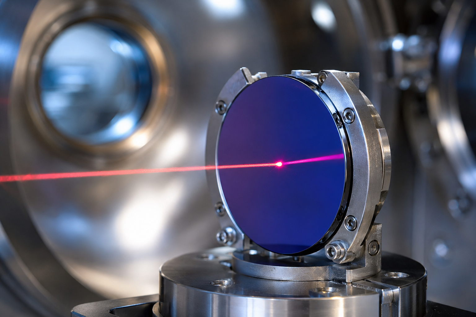
At the frontier of high-power lasers and gravitational wave detection, optical losses are now measured in ppm. We explore how electric field engineering and thermal relaxation push IBS thin films into the single-digit ppm absorption regime, enabling HR mirrors with reflectance up to 99.9966%.

In high-power laser systems, quantum photonics, and interferometric gravitational wave detectors, optical losses (absorption and scattering) at the level of hundredths of a percent are no longer acceptable. Today, managing thin-film quality at the ppm (parts per million) scale has become the absolute industry standard.
When dealing with absorption in the single-digit ppm regime, classical macroscopic material physics gives way to the precise control of microstructural defects, stoichiometry, and electromagnetic field distribution within multilayer dielectric stacks.
Achieving sub-ppm absorption in Ion-Beam Sputtering (IBS) technology requires a synergistic approach combining two fundamental mechanisms:
1. Interference Design: Redistributing Electric Field Profiles
The traditional approach to manufacturing High-Reflection (HR) mirrors relies on simply increasing the number of alternating high- and low-index layers (such as Ta2O5 / SiO2). However, in real-world applications, every added layer introduces cumulative volumetric absorption and interfacial roughness.
Optimizing at the ppm level requires a complete re-engineering of the stack architecture:
• Modifying the thickness profiles of the outermost layers allows engineers to shift the standing wave electric field peaks (the maxima of the E-field) away from high-absorption layer interfaces and boundaries.
• This field redistribution makes it possible to reduce the total layer count (e.g., from 37 down to 31 layers) without sacrificing reflectivity.
• By minimizing the net volume of the absorbing high-index material, total absorption losses are slashed in half, from over 68 ppm down to ~35 ppm, while the net reflectance (R) simultaneously increases.
2. Thermal Relaxation: Eliminating Sub-Stoichiometric Defects
The IBS process is known for producing highly dense, amorphous, and non-porous thin films with exceptional adhesion. However, the high kinetic energy of the sputtered ions inevitably induces localized mechanical stresses and point defects within the deposited tantalum pentoxide (Ta2O5) matrix—primarily oxygen vacancies. These sub-stoichiometric defects act as active absorption centers at the operating laser wavelength (e.g., 1064 nm).
To drive absorption down from tens of ppm into the single-digit ppm regime, a precise post-deposition thermal annealing process must be deployed:
• Standard low-temperature annealing (around 400°C) only partially relaxes internal stresses, leaving residual absorption centers active and trapping absorption levels at approximately 13 ppm.
• Elevating the controlled annealing temperature to 600°C activates oxygen diffusion within the lattice, effectively healing oxygen vacancies and restoring oxide stoichiometry.
• Crucially, this thermal budget is maintained strictly below the crystallization threshold of the film to prevent the formation of grain boundaries, which would otherwise trigger catastrophic scatter loss.
The Result: Optimizing the thermal annealing parameters drives the final measured absorption of a 1064 nm HR mirror down to ~6 ppm, enabling an ultra-stable total reflectance of R = 99.9966%.
Technological Process Control
Maintaining stable, batch-to-batch reproducibility within the single-digit ppm window requires absolute cleanliness of the vacuum environment, suppression of macro-particle generation by the ion source, and automated, real-time optical thickness monitoring. Ultimately, driving absorption down to the ppm scale is the primary catalyst for achieving massive leaps in the Laser-Induced Damage Threshold (LIDT) for demanding continuous-wave (CW) and pulsed petawatt laser applications.
When Every ppm Matters: The Science Behind Low Absorption Optical Coatings | I-Photonics Blog
Read more
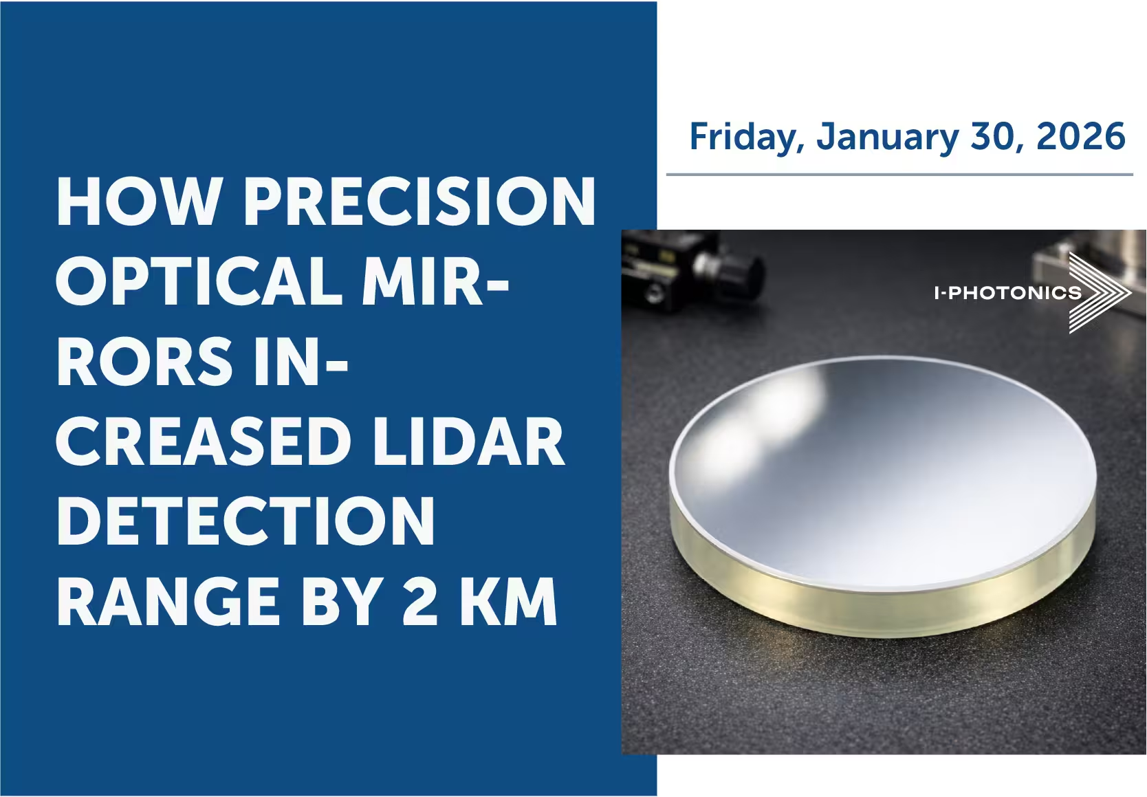
How Precision Optical Mirrors Increased LiDAR Detection Range by 2 km
How precision optics boosts 1550 nm LiDAR range and signal fidelity — a real 13% system improvement case study.
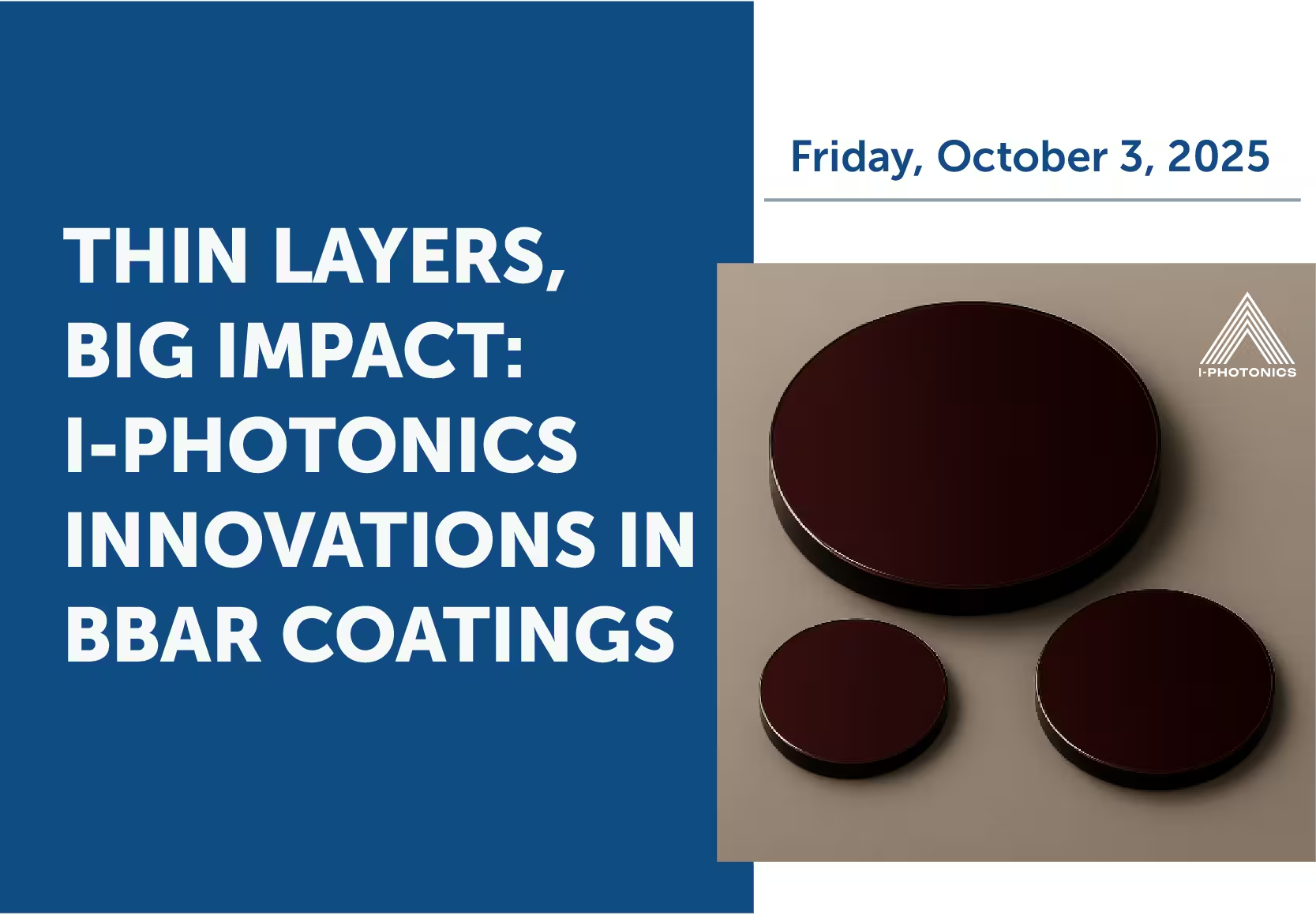
Thin Layers, Big Impact: I-Photonics Innovations in BBAR Coatings
In this edition, we highlight broadband anti-reflection (BBAR) coatings engineered for the critical 8–14 µm LWIR range. By minimizing surface reflections on ZnS and Ge optics, these multilayer coatings achieve transmission levels above 94–98%, unlocking higher sensitivity and performance in thermal imaging, laser systems, and IR sensors.
BBAR Coatings: Thin Layers, Big Impact on Optics | I-Photonics Blog
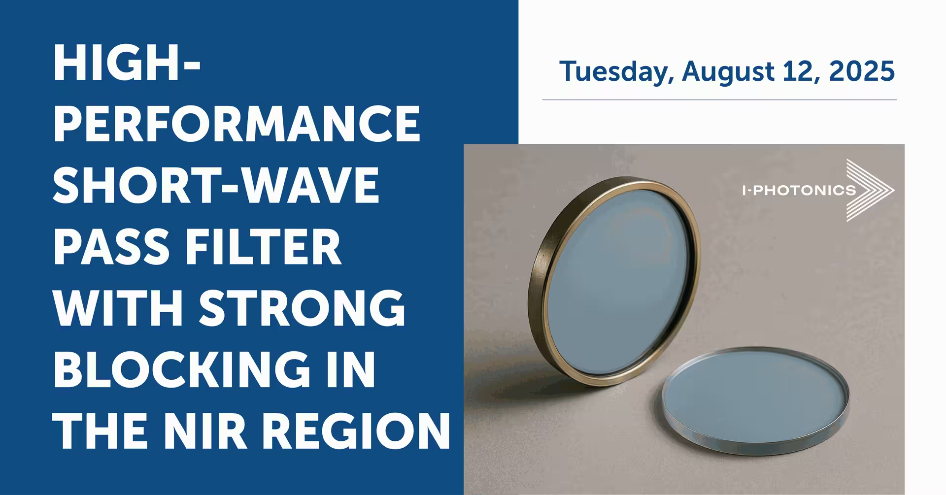
High-Performance Short-Wave Pass Filter with Strong Blocking in the NIR Region
In this edition, we present a cutting-edge short-wave pass filter designed for superior blocking in the near-infrared (NIR) range. Featuring a highly transparent visible passband and ultra-steep edges, this filter enhances contrast and sensitivity for applications like biomedical imaging, laser-induced fluorescence, and precision spectroscopy.